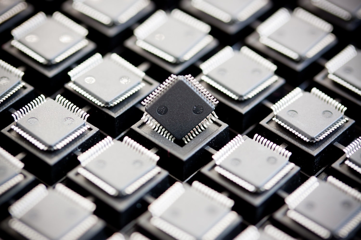
The semiconductor industry offers quite a wide range of technology nodes to sustain the demand for cost reduction as well as for performance increase. So many possibilities that making a choice can be tricky for engineering teams, even if this choice is almost always driven by theCost somehow.
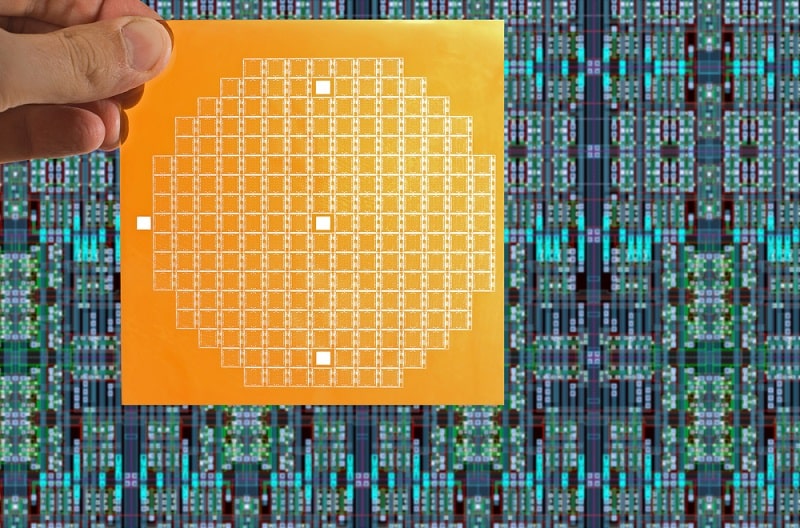
Here, cost means both direct costs such as mask set and wafer costs and hidden costs arising from the reliability of the foundry, the manufacturing process mastery or the yield. Indeed, producing more wafers to get the number of units you need has a price…
Besides Cost, our top 5 criteria when selecting a technology for your ASIC are:
#1 Technology options and mixing possibilities
To reach the targeted performance or level of integration, ASIC designers need to gather different features on the same node. Therefore, Semiconductor foundries offer modular platforms around a core CMOS process, featuring several options (high voltage, image sensor, eFlash, RF, and much more) to capture this demand. They follow two main streams: Moore’s law to improve performances by scaling down geometries (from 40nm to 5nm) and More-than-Moore’s law to increase features for mature nodes (from 1um to 55nm).
#2 IP portfolio
Unfortunately, the technology node itself is not enough; several IP blocks known as standard cells, IO, memories, and others, are required to design an ASIC safely, within a reasonable timeframe, and at a reasonable cost. Indeed, starting with elements that are already functional and qualified allows to focus on more specific parts and increases the success rate on silicon. It is even common that IP blocks such as RF Front-End or MRAM drive the technology node selection and layers to be used.
#3 Reliable simulation models
The two most important criteria for ASIC designers probably are their level of confidence as well as their experience with the simulation models. Beyond the modelling of transistors, one has to pay attention to the accuracy of leakage currents, parasitics (passive or active), and mismatching. Indeed, since manufacturing costs are high, even very high in advanced nodes, ASIC designers know or learn from experience that simulation results must be reliable to commit to performance targets. Designing process-sensitive analog functions with no accurate modelling may result in requiring multiple silicons or significantly reducing the yield.
#4 Quality of service
A Foundry’s quality of service is a key factor to achieve ASIC designs with success. Among those services are the design capabilities (process design kits supporting all major EDA platforms, access to online technical information), the capacity to treat specific requirements (e.g. TI layer adjustment on top metal), and the quality of support provided during the manufacturing process as well as secured planning and quantities.
#5 Final application constraints
Under certain regulations, end-user applications can require a specific location of manufacturing plants or a level of traceability with a specific scrapping procedure. Besides, export forms to be signed with semiconductor foundries should be carefully reviewed before selecting a process node regarding the restrictions listed, depending on the foundry and its location.
To sum up, choosing a technology node is not straightforward. It requires some discussions through the exploration of preliminary ASIC architectures to come to a compromise between the above criteria, without neglecting the cost of course.